Selection Guide of DC/DC Converters for Automotive Navigation Systems
Electronic systems face severe operating challenges under automotive operating conditions, including wide input voltage swings, large transient voltage surges and extreme temperature drift. This article outlines how to design multi-rail power supplies to meet the power demands of different sub-modules in automotive electronic systems amid increasingly stringent performance requirements.
Most mid-to-high-end vehicles currently come factory-equipped with DVD-based GPS navigation systems as standard hardware (Figure 1). However, designing power supplies to regulate the multiple voltage rails within such navigation systems is nearly as complex as developing power solutions for notebook PCs. A typical automotive navigation unit may require six or more independent power rails: 8 V, 5 V, 3.3 V, 2.5 V, 1.5 V and 1.2 V.
The 8 V rail powers the DVD spindle motor for disc rotation, often drawing peak currents up to 2 A.
The 5 V and 3.3 V rails serve as system bus supplies, each rated for 2 A to 3 A continuous output.
The 2.5 V rail feeds memory and I/O peripherals, requiring 1 A to 2 A of supply current.
The 1.5 V and 1.2 V rails deliver core voltage to the CPU and DSP respectively, with power levels ranging from 3 W to 5 W for both rails.
Meanwhile, the growing count of onboard components shrinks available internal enclosure space. Constrained footprint and extended operating temperature ranges make power conversion efficiency a critical design priority, as conventional bulky heat sinks cannot be installed easily.Linear regulators are no longer viable for generating these low-voltage rails at mid-range currents above several hundred milliamps, due to excessive heat dissipation. As a result, switching regulators have gradually replaced linear regulators over recent years, driven primarily by thermal limitations.
Switching power supplies deliver superior efficiency and compact PCB footprint, offsetting drawbacks such as increased circuit complexity and EMI emissions. When selecting switching regulators for automotive navigation systems, devices must satisfy a strict set of key specifications: wide input voltage operating range, high efficiency across full load spectrum, ultra-low quiescent current during normal, standby and shutdown modes, low thermal resistance, and minimal noise & EMI radiation. We elaborate on these core performance requirements in detail below:
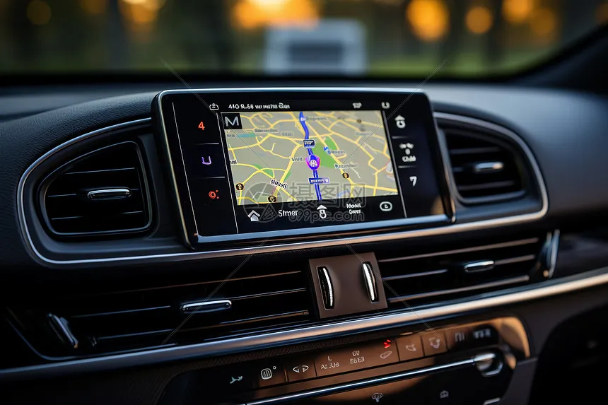
Figure 1: DVD-based GPS navigation systems are standard factory fitments on most mid-to-high-end passenger vehicles
1. Wide Input Operating Voltage Range
All switching regulators must support a wide 3 V to 60 V input operating window to withstand cold-crank voltage drops and load-dump transients. This wide voltage rating enables compatibility with both 14 V and upcoming 42 V automotive electrical architectures.The 60 V maximum input rating provides ample design margin for standard 14 V vehicle systems, which are typically clamped at 36 V–40 V. It also future-proofs designs for next-generation 42 V automotive power networks: circuits engineered for 14 V systems can be upgraded for 42 V platforms without extensive redesign work.
High efficiency across full load profiles is mandatory for nearly all automotive electronics. For instance, a 5 V output converter must maintain ~85% efficiency over a 10 mA to 2.5 A load range. At high output currents, internal power switches must feature low saturation resistance (typically 0.1 Ω at 3 A).To boost light-load efficiency, drive current can be minimized or scaled proportionally to output load current. Internal control circuit power may also be supplied via a bias pin fed from the converter output, a key efficiency advantage of buck regulators. Since bias current is drawn from the output rail instead of the input supply, input draw for control circuitry is reduced by the ratio of output voltage to input voltage.As an example, 100 μA of output-side bias current at 3.3 V translates to only 30 μA of average input current at 12 V. This minimizes standby input power draw and optimizes light-load conversion efficiency.
2. Ultra-Low Quiescent Current
Many automotive subsystems require continuous power even when the vehicle is parked, creating strict low-quiescent-current requirements.The regulator operates in continuous normal switching mode for output currents above ~100 mA. Below this threshold, the device skips switching pulses to maintain regulation and enters a low-power sleep state between pulses, with only essential internal circuitry energized.The converter automatically engages Burst Mode operation under light loads. For a 12 V to 3.3 V buck converter, quiescent current drops below 100 μA in this mode. Internal voltage references and power-good detection circuits remain active during sleep mode to continuously monitor output rail voltage. In full shutdown mode, device quiescent current must fall below 1 μA.
3. Low Thermal Resistance
A low junction-to-case thermal resistance is highly desirable. Devices with exposed bare copper pads on the bottom can be soldered directly to PCB copper planes, which dissipate heat away from the chip. Standard 4-layer PCBs with internal power planes achieve thermal resistance around 40 °C/W. For high-temperature applications with robust thermal coupling to metal housings, typical junction-to-case thermal resistance can reach nearly 10 °C/W, expanding the allowable operating temperature window.
4. Noise & EMI Mitigation Considerations
While switching regulators generate higher noise than linear alternatives, their vastly superior power efficiency makes them indispensable for compact automotive designs. Noise and EMI emissions can be fully controlled as long as the switching device operates with predictable switching behavior.EMI suppression is maximized when the regulator switches at a fixed constant frequency with clean, well-defined switching edges free of voltage overshoot and high-frequency ringing. Small form-factor packages and high switching frequencies support tight, compact PCB layouts that minimize radiated EMI. Additionally, compatibility with low-ESR multilayer ceramic capacitors suppresses input/output voltage ripple, a major secondary source of system noise.
Designing such high-voltage switching regulators poses significant development challenges. Over recent years, Linear Technology has focused heavily on high-voltage DC/DC converter development, building an extensive product portfolio purpose-built to meet rigorous automotive power requirements (Table 1).
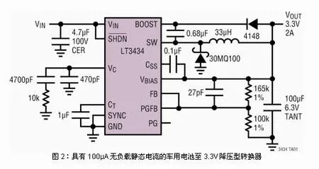
The LT3434 is a recent example of such a DC/DC converter, belonging to an expanding family of monolithic buck switching regulators rated for up to 60 V input. The device addresses all core power design challenges outlined above for automotive navigation hardware.
Wide 3.3 V to 60 V input operating range (Figure 2)
High efficiency delivery at load currents up to 2.5 A
±2% internal reference accuracy across all voltage, load and temperature conditions
Sub-100 μA quiescent current for 12 V to 3.3 V applications via integrated Burst Mode operation
Compact thermally enhanced thin TSSOP package with ultra-low thermal resistance for space-constrained PCB layouts
Current-mode control topology delivering fast transient response and simple external compensation
Proprietary circuitry maintaining constant peak switch current across all duty cycles
Fixed 200 kHz switching frequency with optional external synchronization to higher clock speeds
Precise voltage regulation over full automotive temperature range, integrated Power Good/reset, soft-start and under-voltage lockout (UVLO) protection
This single-chip solution delivers robust, efficient power conversion with minimal PCB footprint for loads up to 2.5 A.
Conclusion
Designing DC/DC power supplies for automotive navigation systems involves complex engineering constraints and strict analog performance standards, but designers no longer need to tackle these challenges from scratch. New generations of dedicated switching regulators from manufacturers including Linear Technology integrate all core functions required to drastically reduce the complexity and engineering workload of automotive power supply development.